Taiwan’s TSMC, the world’s largest semiconductor foundry, is set to build nine new factories this year, continuing its annual tradition of expanding production facilities. This ambitious expansion aims to significantly boost capacity in response to surging demand for advanced processes, including the cutting-edge 3nm (nanometer) technology and the 2nm process slated for mass production by year’s end.
Industry sources reported on Monday that Cliff Hou, TSMC’s Senior Vice President and Deputy Co-Chief Operating Officer (CISO), unveiled plans at the 2025 North America Technology Symposium to construct nine new fabs. This move is designed to support TSMC’s robust growth and meet customer needs. Hou specified eight of these will be wafer fabs, with one dedicated to advanced packaging. The new facilities will span locations in Taiwan, Germany, Japan, and the U.S.
This expansion marks a significant escalation from TSMC’s previous growth patterns. From 2017 to 2020, the company averaged three new fabs annually, increasing to five between 2021 and 2024. For this year’s ambitious plans, TSMC has earmarked between 38 billion USD and 42 billion USD for production capacity expansion.
As TSMC enters the third year of its 3nm process, it anticipates a more than 60% increase in 3nm production capacity compared to last year. The company is also gearing up to commence mass production of its 2nm process by year-end, with plans to implement the 1.6nm process starting late next year.
This rapid expansion is driven by the artificial intelligence (AI) boom, with major fabless semiconductor design customers clamoring for advanced processes to produce AI chips. These chips require higher transistor density to maximize computational power while improving energy efficiency, which is critical for handling the extensive calculations demanded by AI applications.
The impact of this shift is already evident in TSMC’s revenue composition. The 3nm technology’s share of total revenue jumped from a mere 6% in 2023 to 18% last year. By the fourth quarter of 2023, the 3nm process accounted for an impressive 26% of revenue.
On May 13, TSMC made a strategic move to optimize its resources. The company sold mature process equipment to a joint venture in Singapore called VisionPower Semiconductor Manufacturing Company (VSMC), which was formed by its subsidiary Vanguard and Dutch semiconductor firm NXP. This allows TSMC to focus on developing and producing cutting-edge process technology, while Vanguard addresses demand for mature process semiconductors.
On May 16, during a visit to Taiwan for the largest Information Technology (IT) expo, COMPUTEX Taipei, NVIDIA Chief Executive Officer (CEO) Jensen Huang met with TSMC Chairman and CEO Wei Zhe. Huang acknowledged that while TSMC’s advanced processes come at a high cost, they deliver significant value.
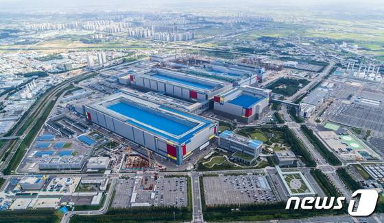
Samsung Electronics faces a critical juncture as it prepares to begin mass production of its 2nm technology in the second half of this year. Failure to secure substantial customer orders could widen the South Korean tech giant’s global market share gap with TSMC. As of Q4 2023, TSMC commanded 67.1% of the foundry market, dwarfing Samsung Electronics’ 8.1% – 59% point difference.
Unlike TSMC’s focused approach, Samsung Electronics operates as an Integrated Device Manufacturer (IDM), juggling memory, foundry, and semiconductor design operations. This diversification presents challenges. While Samsung Electronics invests heavily in foundry facilities at its Pyeongtaek campus, in Taylor, Texas, and Yongin’s semiconductor cluster, it must also maintain substantial annual investments in its core memory business, potentially diluting its focus.
In last month’s Q1 earnings call, Samsung Electronics revealed a shift in strategy for its foundry business. The company prioritized investment in converting existing lines, weighing market conditions and investment efficiency. This approach led to a decrease in investment compared to the previous quarter.
Looking ahead, Samsung Electronics is doubling down on advanced processes. The company is launching mass production of its first-generation 2nm Gate-All-Around (GAA) technology and aggressively pursuing orders for second-generation 2nm customers. Simultaneously, Samsung Electronics aims to bolster its position in mature processes by enhancing specialty process offerings and increasing orders for consumer and automotive products.