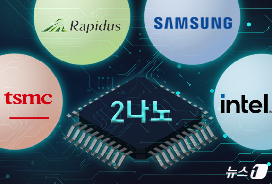
The competition in the 2-nanometer market, widely viewed as the critical battleground for leading foundries, is heating up. Samsung Electronics is doubling down on yield stabilization and customer acquisition to narrow the gap with TSMC. At the same time, American chip giant Intel Corporation has entered the race with its cutting-edge 1.8-nanometer 18A process.
All eyes are on Samsung Electronics as it ramps up efforts in the 2-nanometer foundry market, with industry watchers looking to see whether the company can overcome its recent lackluster performance.
Given Samsung’s initial struggles with low yields in its advanced 3-nanometer process, the company is now laser-focused on ensuring stability in its 2-nanometer technology. Industry analysts suggest that Samsung’s comeback hinges on achieving robust mass production capabilities and yield stability in this crucial 2-nanometer process.
Intel Corporation is rapidly emerging as a formidable competitor, buoyed by investments from Nvidia and substantial U.S. government support. The chipmaker has been steadily improving yields for its 1.8-nanometer 18A process.
According to industry sources and international reports on the 27th, as Samsung strives to catch up with TSMC in 2-nanometer technology, Intel has been making significant progress in improving yields for its advanced 18A process. The 18A node represents Intel’s latest offering, designed to compete directly with TSMC and Samsung’s 2-nanometer processes.
At the RBC Capital Markets Global TMT Conference, Intel confirmed that yields for the 18A process, previously hovering around 10 percent, have been improving by roughly 7 percentage points each month, signaling strong potential for mass production.
Intel has also announced plans to unveil its next-generation Panther Lake chip, built using the 18A process, at CES 2026 in January. With strong U.S. government backing and a 5 billion USD investment from Nvidia, some industry observers argue that this level of support amounts to semiconductor nationalization.
As Samsung Electronics continues to invest heavily in its 2-nanometer process, other foundry players are expected to intensify their efforts to challenge TSMC’s market dominance.
Market research firm TrendForce reports that TSMC currently commands a 70.2 percent share of the global foundry market as of the second quarter. In comparison, Samsung holds 7.3 percent, while Intel remains around 1 percent.
Despite the significant market share gap, industry experts believe there is still room for competition in the 2-nanometer space.
Reports suggest that TSMC has increased wafer prices by up to 50 percent as major clients like Apple and Nvidia cluster around the company, potentially increasing the risk of customer attrition.
Analysts note that if companies like Samsung can ensure process stability, they may attract departing customers with more flexible pricing strategies.
Samsung Electronics is relying on a two-pronged strategy of yield stabilization and customer expansion to regain its competitive edge.
Counterpoint Research projects that Samsung’s 2-nanometer production capacity will rise from 8,000 wafers per month last year to 21,000 wafers per month by the end of next year. Industry sources say Samsung’s 2-nanometer yield has already reached 55-60%.
Samsung’s early adoption of the new GAA (Gate-All-Around) process, which TSMC is only now implementing in its 2-nanometer technology, has given the Korean tech giant valuable experience and a potential competitive advantage. GAA technology significantly reduces current leakage compared to traditional FinFET designs, while substantially improving performance and power efficiency.
Samsung is also ramping up efforts to expand its customer base. The company has already secured five key clients for its 2-nanometer line, including Tesla, Samsung System LSI, MicroBT, Canaan, and Qualcomm Incorporated.
In a major win, Tesla has entrusted Samsung with the production of its 16.5 billion USD autonomous driving AI6 chip, effectively guaranteeing high utilization rates for Samsung’s Texas Taylor plant, set to begin operations in 2027. Tesla CEO Elon Musk’s stated preference for U.S.-based production to mitigate geopolitical risks further underscores Samsung’s regional competitive advantage.
These developments are reflected in improving financial forecasts. Analysts expect Samsung’s non-memory division, which is projected to post losses of 6 to 7 trillion KRW (approximately 4.5 to 5.25 billion USD) this year, to significantly narrow that deficit to between 100 billion and 2 trillion KRW (approximately 75 million to 1.5 billion USD) next year. Some industry watchers even foresee a potential return to profitability by 2027, as Tesla’s chip volumes begin to have a substantial impact.