Hanmi Semiconductor is set to make a significant foray into the U.S. semiconductor market by establishing a local subsidiary, Hanmi USA, in Silicon Valley by year’s end.
The company announced on Friday that it will launch Hanmi USA in San Jose, California, by the end of the year to proactively address U.S. market demands.
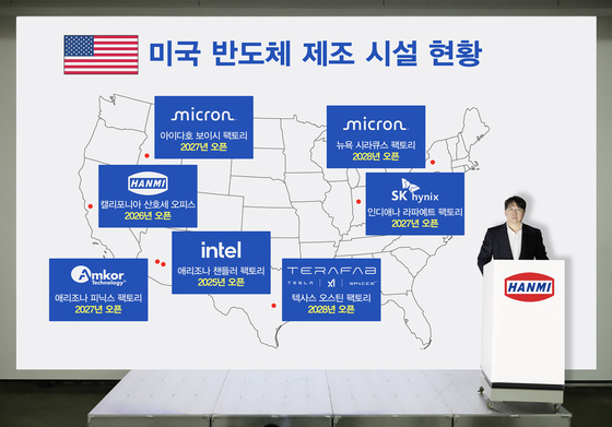
In sync with the operational timelines of new factories from global semiconductor firms, Hanmi plans to deploy seasoned engineers locally and provide hands-on technical support.
Industry giants like Intel Corporation, Micron, Amkor Technology, SK Hynix, and Tesla are accelerating the construction of large-scale artificial intelligence (AI) semiconductor production facilities on U.S. soil, bolstered by support from the CHIPS Act.
Kwak Dong-shin, Chairman of Hanmi Semiconductor, projects a substantial performance boost starting from the second quarter of this year, driven by the persistent surge in global AI semiconductor demand.
With HBM4 production ramping up this year, it’s witnessing a surge in TC bonder orders in the second quarter, a trend that’s expected to intensify in the latter half, Kwak stated. He emphasized that Hanmi Semiconductor’s TC bonders, which currently lead the global market, are poised to reap even greater benefits from the expanding AI semiconductor market.
The establishment of a U.S. subsidiary enables Hanmi Semiconductor to forge direct collaborative ties with global hyperscaler companies, the end-users of their products.
There’s a growing trend among tech giants like Microsoft, Google, Amazon (AWS), and Meta to develop proprietary AI semiconductors, leading to increased direct involvement in reviewing and specifying the high-performance memory and key equipment used in manufacturing processes. This shift is anticipated to drive up demand for packaging equipment tailored for hyperscalers.
Hanmi Semiconductor currently holds the top global market share in thermal compression bonding (TC bonding) equipment, crucial for manufacturing high-bandwidth memory (HBM), a key component in AI semiconductors. To cement its leadership in the next-gen HBM market, the company aims to unveil a prototype of its second-generation hybrid bonder equipment within the year.
The company is also gearing up to supply its 2.5D packaging equipment, including the 2.5D TC Bonder 40 and 2.5D TC Bonder 120, to foundry and the Outsourced Semiconductor Assembly and Test (OSAT) companies this year. The BOC COB Bonder, launched earlier this year as a world-first, has begun shipments to global memory companies and is expected to boost revenue growth alongside rising demand for AI and data centers.
The BOC COB Bonder is a groundbreaking two-in-one bonding machine capable of executing both Board On Chip (BOC) and Chip On Board (COB) processes in a single unit.
In the aerospace sector, a key area for future growth, Hanmi Semiconductor has commenced supplying its EMI Shield 2.0 X series, an electromagnetic interference (EMI) shielding process equipment, to global aerospace firms. The company has maintained market leadership in this niche since its initial release in 2016.
Chairman Kwak stated that its U.S. subsidiary will allow them to provide responsive, on-the-ground support to meet customer needs. As the U.S. emerges as a global semiconductor manufacturing hub, we anticipate securing significant equipment orders alongside new factory operations, driving sustained revenue growth.


