The competition in memory semiconductors is expanding from dynamic random access memory (DRAM)-focused high-bandwidth memory (HBM) to NAND flash. This shift reflects efforts to broaden the use of more cost-effective NAND in response to the surging demand for artificial intelligence (AI) data centers.
This strategy aligns the interests of big tech companies, who can save on investment costs, with memory semiconductor firms aiming to extend their industry supercycle.
Moreover, the race to double HBM’s speed and capacity through innovative structural designs has intensified.
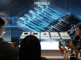
Leading memory manufacturers, including Samsung Electronics, SK Hynix, SanDisk, and Kioxia, unveiled cutting-edge semiconductor technologies and high-performance storage solutions at the Future of Memory and Storage (FMS) 2026, the world’s premier memory and storage event concluding on Thursday. Industry experts view this as the dawn of a new era in semiconductor competition.
Samsung and SK Hynix showcase revolutionary Z-axis and three-dimensional (3D) stacking technologies
The most pressing challenge facing tech giants today is overcoming the memory wall. As AI applications proliferate, processing units like central processing units (CPUs) and graphic processing units (GPUs) are becoming faster. However, the memory responsible for storing and supplying data can’t keep up, leading to overall performance bottlenecks.
No matter how swift the processor, it can’t function optimally if data isn’t delivered at matching speeds. As AI models grow more complex, memory bandwidth and capacity directly impact performance limits.
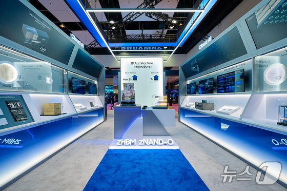
To address this bottleneck, Samsung introduced Z-high-bandwidth memory (HBM). Traditional HBM was positioned adjacent to GPUs or AI accelerators, exchanging data laterally. Despite minimizing the compute-to-memory distance and maximizing bandwidth, a physical gap remained, resulting in significant time and power consumption for data transfer.
ZHBM leverages the Z-axis in addition to the X and Y axes, positioning HBM directly above the GPU to virtually eliminate data travel distance. This next-gen interface system boasts up to eight times the performance and triple the power efficiency of HBM5.
SK Hynix also employed a similar 3D stacking method. Conventional DRAM faced limitations in shrinking cell size on a 2D plane, making capacity increases challenging. 3D stacking allows for significantly higher cell density in the same area, boosting the capacity and density of the main memory tier.
SK Hynix’s 3D stacked DRAM, G0.5, bridges the performance gap between the smaller but faster G0 SRAM and the existing G1 HBM.
NAND’s Renaissance: A Potential Solution to Memory Bottleneck?
NAND has emerged as another key focus at this year’s FMS. While slower than DRAM, its lower cost makes it an attractive option for data center investments. The strategy involves using traditional HBM for operations requiring rapid processing and NAND for less speed-critical tasks.
Memory manufacturers like Samsung and SK Hynix are increasing the number of stacked layers to boost storage density per unit area while reducing per-gigabyte manufacturing costs.
Samsung Electronics reinforced its NAND technology leadership by unveiling the industry’s first 10th generation V-NAND, V10 BV-NAND, featuring over 400 layers. Using wafer bonding and 3-stack technology, they achieved a 58% improvement in memory density compared to the previous generation (V9).
Additionally, Z-NAND-O is a high-performance NAND designed for AI applications, vertically stacking existing NAND chips in four or eight layers using through-silicon-via (TSV) technology.
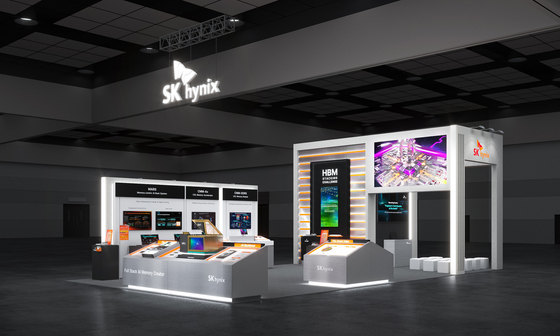
SK Hynix, in collaboration with SanDisk, announced the first standard specification for high-bandwidth NAND flash (HBF), a next-generation storage technology. HBF represents a new memory tier bridging the gap between HBM and solid-state drives (SSDs).
Similar to HBM, HBF employs vertical stacking of eight or sixteen layers, but uses NAND dies instead of DRAM to create ultra-fast, high-capacity flash memory. This technology aims to address the capacity limitations of existing HBM, enhancing AI data storage and retrieval efficiency.
SK Hynix also introduced its 10th generation (V10) 375-layer 4D NAND, currently under development. This product offers 2.5 times better power efficiency than its predecessor. The company plans to begin mass production of high-performance, high-capacity eSSDs using this technology early next year.
Kioxia and SanDisk unveiled a cost-effective AI memory solution, the 332-layer QLC 3D NAND. Traditional Quad-Level Cell (QLC) NAND stores four bits per cell, offering lower cost per capacity but with speed and durability trade-offs.
Like their competitors, these companies aim to overcome QLC limitations by increasing layer count through vertical stacking. They plan to expand into AI data storage and enterprise SSD markets.
Samsung’s One-Stop Solution vs. SK Hynix’s Tiered Memory Approach
The strategies revealed by Samsung Electronics and SK Hynix at FMS 2026 show subtle but significant differences.
Samsung emphasizes its unique position as the only integrated device manufacturer (IDM) capable of providing a comprehensive one-stop solution encompassing memory, logic, foundry services, and packaging.
By offering end-to-end services from product design through manufacturing and packaging, Samsung aims to streamline development cycles while optimizing performance and power efficiency for custom AI semiconductor solutions.
A Samsung spokesperson stated that at FMS 2026, it presented the strategy and roadmap for next-generation AI infrastructure innovation, leveraging the end-to-end solution capabilities. It will continue to strengthen the semiconductor technology leadership in the AI era through differentiated solutions spanning next-gen memory technology, memory, foundry, and advanced packaging.
SK Hynix envisions tiered memory, which integrates diverse memory types into a unified system, as the cornerstone of next-generation AI infrastructure. The company plans to accelerate AI storage ecosystem expansion beyond standard HBM supply through open alliances.
The announcement of the HBF standard specification in partnership with SanDisk at this event, through the Open Compute Project (OCP), the world’s largest open data center technology consortium, aligns with this strategy.
Kim Cheon-seong, head of SK Hynix’s solution development division, remarked that the rapid expansion of AI applications necessitates a fundamental redesign of data processing architectures. Through HBF, it aims to blur the lines between memory and storage, contributing to new system architectures that enhance overall efficiency.