Hanwha Semitech has completed the development of its second-generation hybrid lead bonder, a cutting-edge semiconductor packaging equipment.
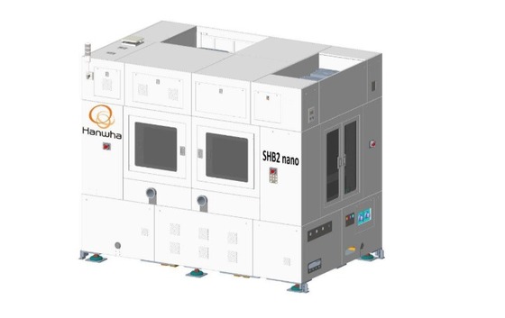
The company announced on Wednesday that it has successfully developed the SHB2 Nano, the latest iteration of its hybrid lead bonder. Hanwha Semitech plans to deliver this advanced equipment to clients for performance testing in the first half of this year. This milestone comes four years after the company supplied its first-generation hybrid lead bonder in 2022.
The hybrid lead bonder is a state-of-the-art packaging device crucial for producing high-bandwidth memory (HBM) used in artificial intelligence (AI) semiconductors. Its innovative technology allows for direct chip-to-chip bonding on copper (Cu) surfaces without the need for bumps. This breakthrough enables the production of ultra-thin, high-density 16-20 layer HBM stacks, significantly boosting data transfer speeds while reducing power consumption.
The newly unveiled SHB2 Nano boasts an impressive alignment precision of 0.1 micrometers (μm) – roughly one-thousandth the width of a human hair. With the second-generation device now complete, Hanwha Semitech is poised to introduce production-ready equipment to the market, building on the success of its first-generation offering.
Alongside its hybrid lead bonder, Hanwha Semitech is expanding its thermal compression (TC) bonder business. The company’s TC bonder, SFM5 Expert, generated over 90 billion KRW (about 63 million USD) in sales last year. In a promising start to this year, the firm has already secured two supply contracts in January and February.
Following the initial delivery of its TC bonder to clients in March last year, Hanwha Semitech saw a marked improvement in its semiconductor division’s performance. This upturn culminated in a return to profitability during the fourth quarter (October to December) of last year.
The company is also making strides in developing its second-generation TC bonder. This new iteration will feature an enlarged bonding head and a fluxless design that minimizes inter-chip spacing. Hanwha Semitech plans to unveil these innovations later this year.
Demonstrating its commitment to innovation, the company has significantly ramped up its research and development (R&D) investments. Last year’s semiconductor-related R&D expenditure saw a substantial increase of over 50% compared to the previous year.
In a strategic move, once Hanwha Group completes its planned restructuring, the tech solutions division will be incorporated under a newly established holding company. This reorganization aims to bolster R&D investments and enhance collaboration among the group’s subsidiaries.
A spokesperson for Hanwha Semitech stated that they’re intensifying the focus on technological advancements to keep pace with the rapidly evolving advanced semiconductor market. Its strategy involves sustained R&D investments to fortify the competitive edge in the industry.