Hanmi Semiconductor revealed on Thursday that it will launch a prototype of its 2nd Generation Hybrid Bonder for next-generation HBM production this year and collaborate with clients.
This strategic move aims to strengthen its position in the TC bonder market for high-bandwidth memory while addressing expected demand for hybrid lead bonding, which is projected to enter mass production by 2029. The company is preparing to begin operations at its hybrid lead bonder factory in the first half of next year.
This strategic move aims to strengthen its position in the TC bonder market for high-bandwidth memory while addressing expected demand for hybrid lead bonding, which is projected to enter mass production by 2029. The company is preparing to begin operations at its hybrid lead bonder factory in the first half of next year.
The firm is closely collaborating with several South Korean semiconductor equipment companies on plasma, cleaning, and deposition technologies for hybrid lead bonding.
Hybrid lead bonding technology directly connects copper wiring between chips and wafers. By eliminating traditional solder bumps, it reduces package thickness while improving heat dissipation and data transfer speeds, making it critical for high-stack HBM with more than 20 layers.
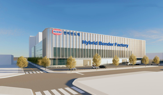
Hanmi Semiconductor is also ramping up infrastructure development for next-generation equipment production. The company is investing about $75 million to build a hybrid lead bonder factory in Incheon’s Juan National Industrial Complex. The two-story facility will span approximately 157,000 square feet, with completion expected in the first half of next year.
The factory will house a state-of-the-art Class 100 cleanroom that meets semiconductor front-end process standards. This advanced facility will employ cutting-edge air conditioning technology to create an ultra-clean environment suitable for nanometer-level precision processes.
Hanmi Semiconductor also plans to reinforce its TC bonder supply. As JEDEC considers relaxing HBM package height standards from 775 to around 900 micrometers, broader adoption of hybrid lead bonding is expected between 2029 and 2030.
A company spokesperson said the firm leveraged its expertise as a leading TC bonder provider for HBM to develop hybrid lead bonder technology, adding that it aims to supply high-quality equipment as customers begin mass production of next-generation HBM.
In the meantime, Hanmi Semiconductor will launch a Wide TC Bonder later this year to meet market demand by increasing HBM die area. This allows for more through-silicon vias and I/O interfaces, expanding memory capacity and bandwidth.


