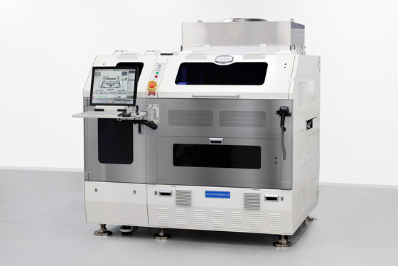
Hanmi Semiconductor announced on June 26 that it will launch its new Flip Chip (FC) Bonder 3.5 equipment for artificial intelligence (AI) system semiconductors and supply it to global foundry and backend (OSAT) companies.
The FC Bonder is an advanced backend processing tool that flips semiconductor chips to directly connect their microscopic bumps to the package substrate. This method shortens the signal transmission path compared to traditional techniques, enabling the production of smaller, thinner high-performance semiconductors with faster data processing capabilities.
Foundries are manufacturing companies that process wafers based on designs from fabless semiconductor firms to produce actual chips. Backend (OSAT) companies package these chips, test their performance, and create finished products for electronic devices.
This new product is Hanmi Semiconductor’s strategic move to enter the 2.5D packaging market for system semiconductors, leveraging its global leadership in TC Bonders for AI memory high-bandwidth memory (HBM). TC Bonders precisely stack and bond individual dynamic random access memory (DRAM) chips vertically using heat and pressure.
In response to the surging demand for AI semiconductors, Hanmi Semiconductor is introducing the FC Bonder 3.5, following last year’s launch of the FC Bonder 75. The company has expanded its product line to support ultra-large dies and multi-chip integration processes crucial for AI semiconductor implementation.
The 2.5D packaging process has become a core technology in AI semiconductors and high-performance computing (HPC), with global tech giants like NVIDIA, AMD, Broadcom, Marvell, and Apple adopting it for their AI chip production.
Hanmi Semiconductor’s FC Bonder 3.5 meets the latest process standards required by global AI semiconductor companies, offering superior productivity and precision compared to competitors. It can handle large panels and substrates up to 340 mm in size using the Chip to Wafer (C2W) bonding method for 2.5D logic dies.
C2W bonding is an advanced packaging technique that precisely bonds individual semiconductor chips directly onto a round wafer before they are cut.
As high-performance AI semiconductors evolve using the Panel Level Package (PLP) method, there’s a trend towards integrating multiple chips like graphic processing units (GPUs), central processing units (CPUs), and HBMs into a single package with a multi-die (chiplet) structure.
PLP is a cutting-edge backend processing technology that packages semiconductor chips on a large rectangular substrate instead of traditional round wafers. This approach minimizes wasted edge space, enhancing production efficiency and playing a crucial role in mass-producing larger, high-performance AI semiconductors at reduced costs.
In AI packaging, 250 mm and 310 mm substrates have become standard. The FC Bonder 3.5 is designed to reliably support customers’ next-generation AI semiconductors in line with this industry trend.
The FC Bonder 3.5 features both flip-chip bonding and face-up (non-flip) bonding capabilities using die attach film (DAF), allowing it to adapt to various process requirements for different customers.
DAF is an ultra-thin solid adhesive film used to attach semiconductor chips to substrates or other chips. Its uniform thickness, unlike liquid adhesives, is advantageous for precise processing. Face-up bonding using DAF secures the chip’s back while keeping the circuit side up, a method crucial for high-density packaging where multiple chips are stacked vertically in confined spaces.
Hanmi Semiconductor plans to significantly enhance its local sales and customer support capabilities by establishing its U.S. subsidiary, Hanmi USA, by year-end. This move, coupled with the expansion of its product lineup, aims to broaden its customer base in the U.S. market, where many global tech giants are based, by supplying both TC Bonders for HBM and equipment for system semiconductors to foundries and backend companies.
A Hanmi Semiconductor spokesperson stated that building on the proven bonding technology for HBM TC Bonders, it aims to make significant sales contributions in the new 2.5D packaging market. It will continue to introduce advanced packaging solutions tailored for the AI semiconductor era.