Samsung Electronics and SK Hynix have unveiled next-generation memory technologies, once again showcasing their industry-leading technological prowess.
As the artificial intelligence (AI) semiconductor market expands from high-performance computing (HPC) to inference applications, both companies are vying to establish dominance in the new memory paradigm. They’re particularly focused on revolutionizing memory structures to overcome existing high-bandwidth memory (HBM) stacking limitations, accelerating efforts to secure leadership in the next-generation AI infrastructure market.
On Wednesday, industry sources reported that Samsung Electronics and SK Hynix presented their innovative memory architectures and next-generation NAND technologies at the Future of Memory and Storage (FMS 2026) event in Santa Clara, California.
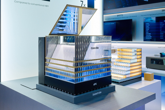
Samsung Electronics Pioneers Memory Structure Innovation with zHBM
Samsung introduced its groundbreaking three-dimensional (3D) memory architecture, zHBM, alongside a new NAND solution dubbed zNAND-O. Unlike traditional designs that place HBM adjacent to AI accelerators, zHBM employs a novel approach by vertically stacking memory directly atop AI accelerators.
This innovative design dramatically reduces the distance between accelerators and memory, minimizing data transfer bottlenecks while boosting both performance and power efficiency.
Samsung claims that zHBM-based systems can achieve up to eight times the performance and triple the power efficiency compared to current HBM5-based systems. The technology also halves thermal resistance, potentially addressing the critical issue of heat management in AI data centers.
Moreover, it enables the integration of customer-specific design circuits (IP) between memory and AI accelerators, allowing tailored designs to meet specific customer needs for capacity expansion and performance optimization. Samsung aims to evolve this into a next-generation platform that synergizes both memory and AI semiconductors.
The zNAND-O solution, unveiled alongside zHBM, features ultra-low-latency NAND technology based on through-silicon via (TSV) 3D packaging. While conventional NAND flash relied on external pathways for data communication, zNAND-O incorporates high-speed elevators (TSV) within the chip itself. This design creates the most direct route for data transfer, enabling ultra-fast performance without delays.
Samsung plans to target various AI inference markets with zNAND-O, focusing on enhancing data loading speeds and responsiveness to boost the performance of AI-enabled devices like personal computers (PCs), smartphones, and robots that operate independently of internet connectivity.
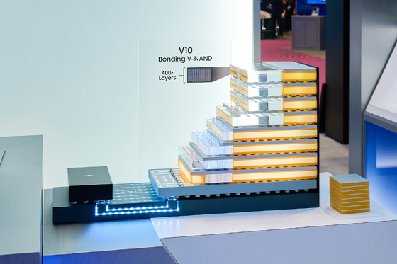
Samsung also debuted its 10th generation V10 BV-NAND, boasting over 400 layers. By implementing wafer bonding and three-stack technology, it increases density by approximately 58% compared to previous generations while enhancing read/write performance and input/output speeds.
The tech giant showcased an impressive array of memory products for AI data centers, including HBM4E, next-generation HBM5, LPDDR5X-PIM, and enterprise SSDs, demonstrating its unrivaled competitiveness across dynamic random access memory (DRAM), NAND, and storage sectors.
SK Hynix Unveils HBF as the Next Frontier After HBM
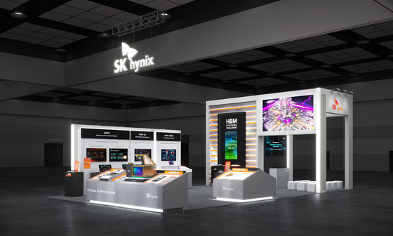
SK Hynix introduced its new memory layer, High Bandwidth Flash (HBF), positioning it as the successor to HBM in the AI market. HBF acts as a bridge between HBM and NAND-based storage, aiming to combine NAND’s vast storage capacity with data transfer speeds surpassing traditional flash.
Industry experts note that the exponential growth in data processing demands, driven by the proliferation of AI inference services, has exposed capacity and cost limitations when relying solely on HBM. HBF is seen as a key technology for implementing a tiered memory structure that processes frequently accessed data with HBM while managing large data volumes with HBF. This approach is expected to maximize the use of relatively cost-effective NAND flash memory, thereby reducing overall system costs.
The previous memory hierarchy consisted of SRAM, HBM, and NAND. The new AI architecture may evolve to include SRAM, HBM, HBF, and high-capacity NAND, potentially boosting overall system performance and cost efficiency simultaneously.
During the event, SK Hynix also revealed the first standard specifications for HBF, developed in partnership with SanDisk. It supports capacities up to 512 gigabytes (GB) and data transfer speeds of up to 3 terabytes (TB) per second. Designed with the semiconductor standard connection specification UCIe-based open interface, it can integrate with various AI processors, including graphic processing units (GPUs) and central processing units (CPUs). The company is also spearheading ecosystem expansion through a consortium involving tech giants like Google and Tenstorrent.
SK Hynix further showcased its next-generation 375-layer 4D NAND, boasting a 2.5 times improvement in power-to-performance ratio compared to its predecessor. The company aims to commence mass production of high-performance enterprise SSDs utilizing this technology in early 2027.
Ushering in the Era of AI Memory Architecture Beyond HBM Competition
Industry analysts believe that FMS 2026 marks a paradigm shift in AI memory competition. While previous focus centered on HBM layer count and bandwidth competition, the future battleground will be AI Memory Architecture – the ability to efficiently connect memory and AI chips while optimizing DRAM, NAND, and storage into a cohesive tiered structure.
AI Memory Architecture encompasses the overarching operational rules and blueprints within semiconductor or computer systems, governing how chips, memory, and software exchange data and perform computations. This holistic approach not only addresses component construction but ensures the entire system operates with maximum speed and energy efficiency.
As the industry transitions from generative AI to agentic and physical AI, the volume of data processed by AI infrastructure is skyrocketing. This trend underscores the critical importance of technologies that not only enhance memory performance but also optimize power efficiency, heat management, and scalability in future semiconductor markets.
An industry insider remarked that Samsung Electronics has proposed a next-generation memory vision through its 3D-stacked zHBM, while SK Hynix has introduced HBF as a tiered memory solution. The future competitive landscape will hinge not just on developing faster memory, but on how effectively memory architectures can enhance the efficiency of entire AI systems.