

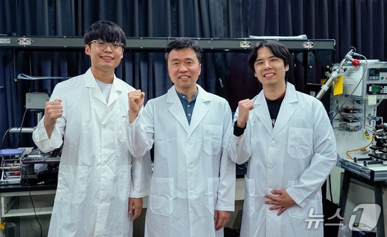
Gwangju Institute of Science and Technology (GIST) announced on Tuesday that a research team led by Professor Seol Jae Hun from the Department of Mechanical Robotics Engineering has developed a groundbreaking process technology. This innovation allows for the acquisition of high-purity two-dimensional materials without external contamination, enabling precise manipulation.
Two-dimensional materials like graphene and molybdenum disulfide (MoS2) possess unique physical properties, making them subjects of research in various fields including electronics, optics, and energy. However, their extreme thinness and sensitivity mean that even minor impurities or mechanical damage during production can significantly degrade their properties.
The research team successfully obtained pure two-dimensional material flakes without impurities, using MoS2, a widely used two-dimensional material in electronic devices.
They developed a novel process technology that allows for precise operations such as adhering, flipping, and stacking without using polymer materials. This technique leverages the Van der Waals forces that act between identical materials.
The two-dimensional materials processed through this new method maintained an exceptionally clean state, free from residues, defects, oxidation, and mechanical deformation. They also demonstrated outstanding results in electrical performance tests.
Professor Seol emphasized the significance of the research, noting that the breakthrough could pave the way for the flexible creation of customized device structures using a variety of two-dimensional materials, all while maintaining their inherent properties. He added that this advancement is expected to significantly improve the performance of electronic and optoelectronic devices based on two-dimensional materials in the future.
This groundbreaking research, guided by Professor Seol and conducted by doctoral student Lee Min-young and integrated master’s and doctoral student Kim Chang-ho, was published online on April 2 in the prestigious international journal, Advanced Materials, in the field of materials science.