Korea Advanced Institute of Science & Technology (KAIST) Professor Kwon Ji-min and his research team have made a groundbreaking announcement on Thursday. They’ve successfully automated the selection of two-dimensional (2D) semiconductors using artificial intelligence (AI) technology, leading to large-scale transistor production and analysis. This innovative research was a collaborative effort involving Ulsan National Institute of Science & Technology (UNIST), National Hanbat University, Hanyang University, and Washington University in St. Louis.
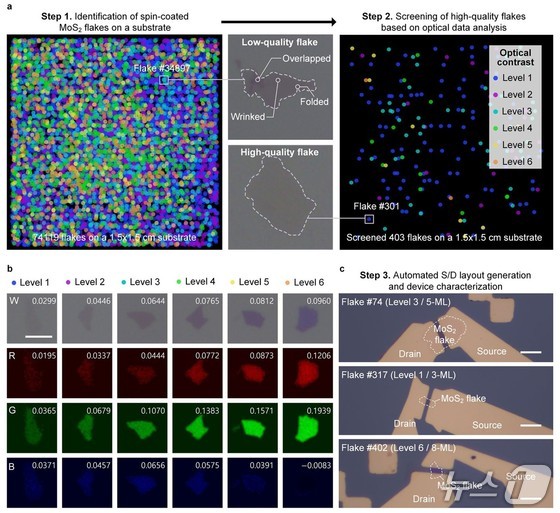
2D semiconductors, ultra-thin materials consisting of just a few atomic layers, are emerging as crucial components for next-generation AI semiconductors and ultra-low-power devices. The team’s novel approach leverages red,green and blue (RGB) brightness differences in optical microscope images, enabling AI to automatically identify desired semiconductors and streamline electrode design.
From over 120,000 samples, the researchers selected suitable specimens to produce and analyze 1,615 transistors. Their findings revealed a previously undocumented correlation: while thicker semiconductors improved current flow, they simultaneously decreased switching performance.
This study marks a paradigm shift in 2D semiconductor research, transitioning from experience-based methods to data-driven approaches. The team’s work paves the way for predicting semiconductor performance using optical microscope images and sets the stage for AI-supported design innovations.

The implications of this research are far-reaching, particularly for next-generation logic and memory 2D semiconductor devices. By producing and measuring large quantities of uniformly thick devices, researchers can systematically address issues such as device dispersion, contact characteristics, and thickness-dependent transport. The wealth of statistical data generated enables the development of data-driven compact models that account for thickness-dependent properties and variations. This advancement is expected to significantly improve the accuracy of circuit-level simulations, accelerating the practical application of 2D devices.
Professor Kwon emphasized that this research has automated both semiconductor selection and production processes, laying a solid foundation for rapid development of next-generation semiconductors.
This groundbreaking study received support from the Ministry of Science and Information and Communications Technology (ICT), the National Research Foundation of Korea, and the Ministry of Trade, Industry and Energy. The findings were published on April 3 in the prestigious international materials science journal, Advanced Functional Materials.