Despite numerous experimental attempts, the desired results remained elusive. Adopting the mindset that the problem often lies in the fundamentals, it revisited key parameters such as pressure, temperature, equipment power, and gas flow rates. This approach ultimately led to a breakthrough.
Even for a semiconductor engineer with 26 years of experience, developing a 4-nanometer ultra-low-power process posed a significant challenge. After multiple failed experiments, it decided to reexamine the most basic variables of the process. The resulting technology became the cornerstone for the base die in Samsung Electronics’ next-generation high-bandwidth memory (HBM), HBM4.
According to Samsung Electronics’ semiconductor newsroom on Thursday, Choi Jung-min, Project Leader (PL) in the Foundry Technology Development Division, revealed the development process behind the 4-nanometer ultra-low-power process technology used in the HBM4 base die during a newsroom interview.
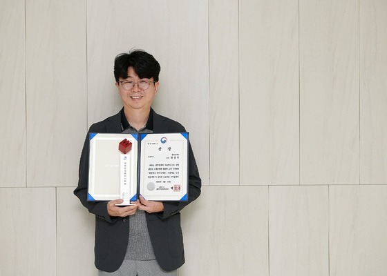
In recognition of his technological achievements, Choi received the Korean Engineer Award in March, an honor presented by the Ministry of Science and Information and Communications Technology (ICT) and organized by the Korea Industrial Technology Association.
The core innovation led by Choi focuses on reducing power consumption while enhancing performance. As artificial intelligence (AI) semiconductors face exponentially growing data processing demands, technologies that minimize power consumption and heat generation have become critical competitive advantages.
To achieve this, Choi optimized both process and design by lowering the height of Fin Field-Effect Transistor (FinFET) structures and reducing the width of contacts connecting internal components.
This approach reduces power consumption by lowering the capacitance – the unnecessary charge stored within the semiconductor. By optimizing various contact structures, Choi’s team improved both power efficiency and overall performance.
This groundbreaking technology has been implemented in Samsung’s HBM4 base die.
HBM is a high-performance memory that vertically stacks multiple dynamic random access memory (DRAM) chips to boost data processing speeds. The base die, positioned at the bottom of these stacked DRAMs, interfaces with graphics processing units (GPUs) or AI accelerators, managing data, power, and control signals. It essentially functions as a traffic control center, orchestrating data flow between multiple DRAM layers and AI semiconductors.
With HBM4’s increased data processing requirements and the base die’s more complex functions, the importance of advanced foundry processes has grown significantly. This is crucial for enabling rapid data exchange while minimizing power consumption.
Choi explained that by proactively implementing the 4-nanometer ultra-low-power process technology, it contributed to the development and mass production of the HBM4 base die. This technology allowed us to significantly increase data processing speeds.
Samsung Electronics has become the first in the world to mass-produce HBM4 base dies using its proprietary 4-nanometer ultra-low-power process. The company’s ability to produce these base dies in-house stems from its unique position of having both memory and foundry operations. This integration – from DRAM production for HBM to advanced foundry processes for base die creation and packaging – is considered a major competitive advantage.
The 4-nanometer process is also viewed as a key driver for the recovery of Samsung’s foundry business. Industry analysts report that the utilization rate of Samsung’s 4-nanometer process has risen significantly, driven by increased demand for HBM base dies and AI inference semiconductors.
As the AI market continues to expand, demand for HBM and custom AI semiconductors (ASICs) is expected to grow, further underscoring the importance of advanced foundry processes.
Choi joined Samsung Electronics’ memory division in 2001, where he was responsible for developing and mass-producing high-speed SRAM products. He transferred to the foundry division in late 2008 and has since overseen logic semiconductor process development and mass production, from 45-nanometer to the current 4-nanometer technology.
Drawing on his 26 years of field experience, Choi emphasized the importance of collaboration with colleagues. He stated that it views this award not as a personal achievement, but as a meaningful recognition of the entire team’s collective efforts and perseverance through numerous challenges.