

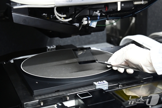
The Electronics and Telecommunications Research Institute (ETRI) announced on Thursday that it has successfully developed ultra-high-resolution Light Emitting Diodes on Silicon (LEDOS) displays, a key technology for the artificial intelligence (AI) and extended reality (XR) era, along with the ultra-precise laser bonding technique required for their implementation.
This breakthrough has garnered attention for its ultra-high-density bonding technology, which reliably connects over 920,000 bumps in a 10µm pitch environment. This achievement significantly surpasses the existing AI semiconductor packaging technology, HBM4 (20µm pitch, 200,000 bumps), delivering superior integration density through a cost-effective process.
The research team employed a laser-based simultaneous transfer and bonding process using their proprietary material, SITRAB. This innovative approach minimizes fine contaminant generation during bonding, thanks to its fume-less characteristics, while the room-temperature stage process reduces substrate deformation and alignment errors.
Using this technology, the team successfully bonded GaN-based micro LED chips onto silicon Complementary Metal-Oxide-Semiconductor (CMOS) circuits, achieving a 2500 PPI ultra-high-resolution LEDOS display.
LEDOS enables the direct arrangement of ultra-small micro LEDs on silicon wafers, paving the way for ultra-high-resolution, high-brightness, and low-power displays in XR devices such as augenmented reality (AR) glasses and virtual reality (VR) headsets.
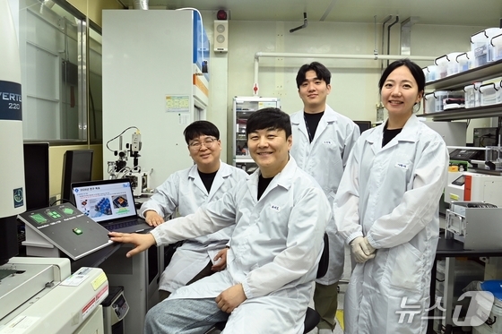
The findings were published in the May 11 issue of the journal Microsystems & Nanoengineering. The technology is currently being transferred to domestic material and equipment companies for mass production verification in semiconductor back-end processing lines.
Dr. Joo Ji-ho, head of ETRI’s Low-Carbon Integrated Technology Research Lab, stated that securing ultra-precise bonding technology for ultra-high-resolution displays is crucial in the AI and XR era. LEDOS technology has the potential to evolve into a next-generation high-density heterogeneous integration platform.
Dr. Choi Kwang-Seong, director of the Creative Source Research Division, emphasized that this achievement demonstrates ultra-high-density bonding that surpasses HBM4 using domestic materials and processes. It is poised to lead the market for AR and VR devices, as well as advanced semiconductor packaging.