Samsung Electronics has launched the world’s first shipment of HBM4E samples, marking its entry into the next-generation semiconductor market. SK hynix has also accelerated its product supply schedule, originally planned for the second half of this year, and has begun shipping HBM4E samples, setting the stage for fierce competition between the two companies.
The key turning point in the HBM4E race is expected to be the post-processing technology and customer validation results. Samsung plans to implement a new technology called hybrid bonding starting from 16-layer products. SK hynix aims to highlight stability by adopting its proven Advanced Mass Reflow-Molded Underfill (MR-MUF) process.
The final supply volume will likely be determined by the actual performance of these chips in customer products. As high-bandwidth memory (HBM) is a custom semiconductor, the company that best optimizes performance and heat control for major tech clients like NVIDIA is expected to come out on top.
Samsung Bets on Hybrid Bonding After World-First Shipment; SK Counters with MR-MUF Technology
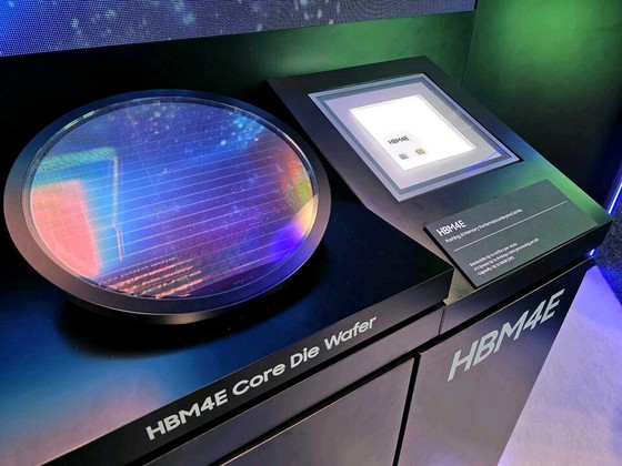
Industry sources reported on Tuesday that Samsung Electronics unveiled the technical specifications of its HBM4E 12-layer product on May 29 and announced sample shipments to customers. The new product combines 1c nano dynamic random access memory (DRAM) for memory functions with a base die using Samsung’s 4-nanometer process for logic operations.
This cutting-edge product achieves an impressive input/output speed of up to 16 Gbps and a bandwidth of 4 TB/s per stack, meeting the high-capacity data processing demands of next-generation artificial intelligence (AI) systems.
Samsung plans to introduce its innovative hybrid bonding process starting with the 16-layer product line. This next-gen packaging technology eliminates fine protrusions between chips and directly bonds copper wiring, creating tightly connected data pathways. The result is a thin chip profile with maximized data processing speed and energy efficiency.
By leveraging this technology, Samsung aims to gain an edge in thickness and thermal management, positioning itself as a technical leader for products with 16 or more layers.
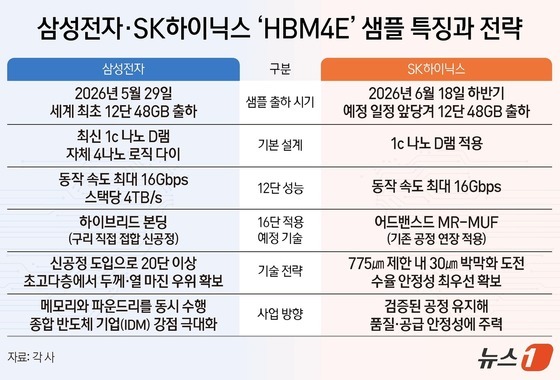
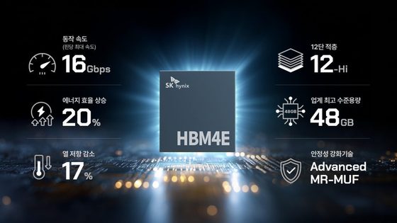
SK hynix, not to be outdone, supplied HBM4E 12-layer samples on the 18th of this month, significantly ahead of its initial schedule set for the second half of the year.
The company’s core mass production strategy focuses on yield stabilization using proven technology. SK hynix plans to stick with its existing Advanced MR-MUF process up to 16 layers to minimize uncertainties in early production stages.
The Advanced MR-MUF process is SK hynix’s proprietary HBM packaging technology. It involves stacking multiple chips and injecting a liquid protective material into the gaps, solidifying them simultaneously. This method excels in heat dissipation and effectively controls chip warping, crucial for the stable mass production of high-layer HBM products exceeding 12 layers.
SK hynix is tackling the challenge of stacking 16 layers within the 775-micrometer (775㎛) package thickness limit set by JEDEC. The company is currently refining its thin-film processes to reduce DRAM wafers to approximately 30㎛.
Song Myung-seop, an analyst at iM Securities, commented that the 16-layer certification will likely pit Samsung’s new hybrid bonding process against SK hynix’s proven MR-MUF extension. In the short term, SK hynix’s MR-MUF may have a stability advantage, while in the long run, Samsung’s early investments in hybrid bonding could pay off, creating an intriguing risk landscape.
Custom Memory Market: Client-Specific Optimization is Key
The final order volume for next-gen HBM will likely hinge on validation test results from major tech clients. Actual performance in client systems will be the crucial metric, rather than manufacturer-announced specs.
Heat management during intensive data processing and power efficiency will be decisive factors for adoption. Unlike traditional DRAM, which focused on standardized products, HBM is highly customized to meet specific client needs.
Even after initial specs are set, performance may vary or improve during client system optimization, making final yield and compatibility critical.
Kim Yang-pyung, a senior researcher at the Korea Institute for Industrial Economics & Trade, noted that market challengers must emphasize their products’ superiority in specific areas compared to industry leaders. Even after specs are disclosed, adjustments will be made to meet client demands. Ultimately, aligning with client expectations and achieving overall system harmony is key.
Wafers Shift to HBM, Deepening Supply Shortage in DRAM Market
The tech race between Samsung and SK hynix is reshaping the memory semiconductor market’s supply landscape. Surging AI demand has prioritized HBM production, exacerbating the general-purpose DRAM shortage.
Industry forecasts suggest HBM’s share of total DRAM wafer input will rise from 22% this year to 30% by 2027. However, HBM’s share of total bit supply is expected to reach only 9% in 2026 and 13% in 2027.
Total memory bit supply refers to the overall data storage capacity of memory semiconductors supplied to the market. The discrepancy between input and output shares is due to the high number of wafers discarded during HBM production.
As HBM production ramps up, fewer wafers will be available for general DRAM, likely leading to supply shortages. An industry insider remarked that strong HBM prices will drive major memory companies to allocate more capacity to HBM production. This will further constrain general-purpose DRAM supply, significantly boosting manufacturers’ overall memory price negotiation power.
As HBM production increases, fewer wafers will be available for general DRAM, likely leading to supply shortages. An industry insider remarked that the stronger HBM prices remain, the more capacity major memory companies will allocate to HBM production, adding that this will further constrain general-purpose DRAM supply, significantly boosting manufacturers’ overall memory price negotiation power.