The competition in artificial intelligence (AI) semiconductor technology is expanding beyond miniaturization to advanced packaging. The key to AI chip performance and energy efficiency now lies in how quickly and efficiently graphic processing units (GPUs) can be connected to high-bandwidth memory (HBM).
As global semiconductor firms ramp up investments in advanced packaging and testing capabilities, new growth opportunities are emerging in the materials, components, and equipment sector. This shift marks an expansion of the semiconductor investment race from front-end to back-end processes.
Global Chipmakers Accelerate Advanced Packaging Investments
Industry sources reported on Monady that capital investments to meet rising AI chip demand are spreading across foundries, back-end specialists (OSATs), and memory manufacturers. Notably, there’s a surge in investments to boost advanced packaging and testing capacity.
TSMC, the world’s largest foundry, maintained its 2026 capital expenditure (CAPEX) forecast at 60-64 billion USD in its Q3 earnings call on October 15. This reaffirms TSMC’s aggressive investment strategy to meet growing AI chip demand, following an upward revision in Q2.
TSMC plans to allocate 10-20% of its capex to advanced packaging, testing, and photomask production. Expanding capacity for Chip on Wafer on Substrate (CoWoS), which integrates GPUs and HBM into a single package, is a top priority.
Hanwha Investment & Securities noted that TSMC recently cited supply shortages in both CoWoS technology and some testing equipment, necessitating further investment. The firm observed that front-end wafer capacity expansion is naturally driving increases in CoWoS and testing capacity.
As TSMC’s CoWoS capacity remains constrained, Intel Corporation’s Embedded Multi-die Interconnect Bridge (EMIB) technology is gaining attention as an alternative. EMIB uses small silicon bridges embedded in the package substrate to connect chips at high density.
Global OSATs are also boosting investments. Taiwan’s ASE upped its 2026 capex plan from 8.5 billion USD to 10.5 billion USD in July, accelerating capacity expansion as demand for advanced packaging and testing of high-performance chips surpassed expectations.
In September, U.S.-based Amkor announced phase two of its Arizona advanced packaging and testing campus expansion, increasing total planned investment to about 12 billion USD. The company aims to establish local advanced packaging, wafer bumping, inspection, and testing capabilities to serve the AI chip supply chain.
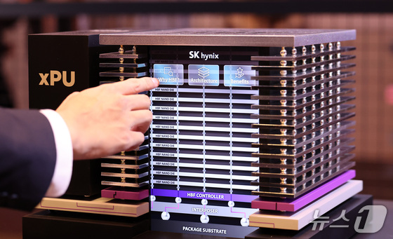
Samsung, SK hynix, and Micron expand HBM back-end operations globally Memory manufacturers are simultaneously expanding production capacity and back-end facilities to meet surging HBM demand.
Samsung Electronics operates back-end facilities in Onyang and Cheonan, South Korea, and Chongqing, China. Daishin Securities expects Samsung to boost advanced packaging investments and research and development (R&D) in Onyang while expanding HBM back-end capacity in Cheonan.
In Vietnam, efforts are underway to secure additional semiconductor final testing facilities, likely to diversify the back-end production network while complementing existing sites.
SK hynix is expanding HBM and advanced packaging capacity in Cheongju, South Korea, and Indiana, USA.
In West Lafayette, Indiana, the company is building HBM advanced packaging facilities and R&D centers. Following a groundbreaking ceremony in August, mass production is slated to begin by late 2029. In South Korea, SK hynix is meeting rising demand by expanding HBM production facilities and leveraging back-end outsourcing.
Micron is investing about 7 billion USD in Singapore to construct HBM advanced packaging facilities. Operations are set to begin this year, with significant contributions to HBM supply expected from 2027.
As foundries and memory makers ramp up advanced packaging investments, the AI chip production race is expanding beyond wafer manufacturing to chip assembly, interconnection, inspection, and testing.
GPU-HBM interconnect tech crucial for AI performance; bonding, inspection, and test equipment makers poised to benefit Advanced packaging is gaining prominence as AI chip performance enhancement strategies evolve.
The semiconductor industry has long focused on shrinking circuit line widths to pack more transistors into the same area. However, as manufacturing complexity and capital costs rise with advanced nodes, the limits of relying solely on miniaturization for performance and efficiency gains are becoming apparent.
For AI chips, data transfer speed between GPUs and memory is as crucial as raw computational power. Even with high-performance processors, overall system performance can be bottlenecked by insufficient memory bandwidth.
Consequently, advanced packaging techniques that minimize data transfer bottlenecks between GPUs and HBM, enabling multiple chips to function as a unified system, are becoming increasingly vital.
Advanced packaging technologies densely interconnect chips with diverse functions or stack them vertically into a single package. This approach can boost data transfer speeds and energy efficiency independently of circuit miniaturization.
Notable examples include TSMC’s CoWoS and Intel Corporation’s EMIB, which are 2.5D packaging technologies that horizontally connect multiple chips. HBM employs 3D stacking for DRAM chips, which are then linked to GPUs using technologies like CoWoS.
French market research firm Yole Group projects the global advanced packaging market to more than double from $55 billion in 2025 to over $120 billion by 2031.
Yole anticipates advanced packaging will account for over half of total semiconductor packaging revenue by 2031. The firm notes that pricing power is concentrated in areas with high entry barriers, such as AI chip packaging, HBM packaging, memory testing, and advanced substrate technology, alongside production capacity.
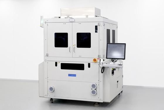
As packaging technology advances, demand for related equipment is set to rise. HBM manufacturing requires precise stacking and bonding of thin DRAM dies, with thermal compression (TC) bonders playing a key role. As stack heights increase and chips thin, bonding precision and yield management become increasingly critical.
Advanced packaging processes also emphasize bumping, redistribution, and high-density substrate technologies for chip interconnection. As chip connections become more precise, even minor bonding defects or alignment errors can significantly impact product performance and yield.
Consequently, demand is expected to grow for inspection and measurement equipment to verify bonding quality and internal package defects, as well as for testing equipment to validate completed semiconductor performance.
Unlike wafer manufacturing inspection tools, advanced packaging requires various quality checks after stacking, bonding, and package completion. This indicates new equipment demand arising not just from capacity expansion, but also from increased process complexity.
Domestic materials, components, and equipment firms are poised for new opportunities. Growth is anticipated in demand for HBM bonding equipment, packaging inspection and measurement tools, testing equipment, and related materials.
Daishin Securities notes that as back-end processes gain strategic importance, investments are emerging in both new facilities and the conversion of aging front-end lines, benefiting the domestic back-end value chain.
Hanwha Investment & Securities advises focusing on emerging equipment and outsourcing demand driven by evolving production methods in back-end processes, rather than just increased production volume.